TL;DR

Get the latest gadgets delivered free with Prime
- Fast, free delivery on millions of items
- Prime Video, Amazon Music and more included
- Member-only deals all year
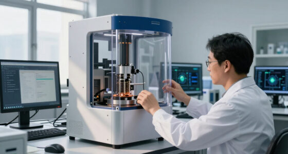
Xanadu and Mitsubishi Chemical have announced a joint effort to develop quantum computing solutions for EUV lithography. The collaboration aims to address challenges in semiconductor manufacturing, with confirmed progress in research and prototype testing. The impact could be significant for future chip production, though practical applications are still in early stages.
Xanadu and Mitsubishi Chemical have jointly announced a collaboration to develop quantum computing solutions aimed at enhancing extreme ultraviolet (EUV) lithography processes. This partnership seeks to leverage quantum technology to address key challenges in semiconductor manufacturing, a sector critical for advancing computing power and chip miniaturization. The announcement underscores a growing interest in applying quantum computing beyond traditional fields, targeting industrial-scale applications with potential impacts on chip quality and production efficiency.
According to the announcement, Xanadu, a leading quantum computing firm based in Toronto, and Mitsubishi Chemical, a major Japanese chemical and materials company, are working together to integrate quantum algorithms into EUV lithography processes. The collaboration has already achieved preliminary results, including the development of prototype quantum algorithms that could optimize the complex light patterning used in chip fabrication. Xanadu’s quantum hardware, which employs photonic qubits, is being tested for its ability to simulate and improve the precision of EUV light sources, which are critical for producing smaller, more powerful semiconductors. Mitsubishi Chemical provides expertise in materials and chemical processes, aiming to adapt quantum solutions to the specific needs of EUV mask design and process control. While the partnership is still in early research phases, both companies have expressed optimism about the potential for quantum computing to reduce defects and increase yield in chip manufacturing, which faces ongoing challenges due to the complexity of EUV lithography at advanced nodes.Officials from Xanadu and Mitsubishi Chemical emphasized that this initiative is part of a broader effort to explore quantum applications in industrial settings. The collaboration has secured initial funding and is expected to progress through pilot testing over the next 12 to 18 months, with plans to evaluate the scalability of quantum-enhanced lithography techniques in real-world manufacturing environments.
Potential Impact of Quantum Tech on Semiconductor Manufacturing
This collaboration could mark a significant step in applying quantum computing to industrial processes, specifically in EUV lithography, which is essential for producing next-generation semiconductors. If successful, quantum algorithms could help optimize the complex light patterns used in chip fabrication, potentially reducing defects, increasing yield, and enabling further miniaturization of chips. The development aligns with broader industry efforts to incorporate advanced computing technologies to overcome current manufacturing bottlenecks, which could lead to faster innovation cycles and more powerful, energy-efficient electronics. However, the practical deployment of quantum-enhanced lithography remains at an early stage, and it is not yet clear when or if these solutions will be commercially viable at scale.
quantum computing hardware for industrial applications
As an affiliate, we earn on qualifying purchases.
As an affiliate, we earn on qualifying purchases.
Quantum Computing’s Emerging Role in Semiconductor Tech
Quantum computing has been primarily viewed as a tool for cryptography, optimization, and simulation in research settings. Recently, industry leaders have begun exploring its potential for practical applications in manufacturing, especially in areas requiring complex patterning and process control. Xanadu, known for its photonic quantum hardware, has been active in developing algorithms for material science and optimization tasks. Mitsubishi Chemical, with a history rooted in chemical and material innovation, has shown interest in applying advanced computing to improve manufacturing precision. The collaboration builds on these developments, aiming to pioneer quantum solutions tailored for EUV lithography—a critical process in the production of cutting-edge semiconductors. The challenge lies in adapting quantum algorithms to real-world manufacturing conditions and scaling them for industrial use, which remains a work in progress.
“Our goal is to leverage quantum technology to enhance the precision and efficiency of EUV lithography, addressing key challenges in chip manufacturing.”
— Mitsubishi Chemical spokesperson
EUV lithography optimization tools
As an affiliate, we earn on qualifying purchases.
As an affiliate, we earn on qualifying purchases.
Early-Stage Development and Commercial Viability
While preliminary results are promising, it is still unclear when quantum-enhanced EUV lithography will be ready for commercial deployment. The research is in early phases, with pilot testing scheduled over the next year, and scalability remains a key challenge. Experts caution that quantum hardware stability and integration into existing manufacturing lines will require significant further development. Additionally, it is uncertain whether the benefits observed in lab settings will translate effectively to large-scale production environments, or whether cost and complexity will limit adoption in the near term.
As an affiliate, we earn on qualifying purchases.
Next Steps in Testing and Scaling Quantum Solutions
Both companies plan to continue pilot testing of quantum algorithms for EUV lithography over the next 12 to 18 months. The focus will be on validating improvements in process accuracy and defect reduction in controlled environments. If successful, the partnership aims to develop scalable prototypes suitable for industrial implementation, potentially leading to pilot programs in semiconductor fabs. Further research will also explore integrating quantum hardware directly into existing manufacturing workflows, with the goal of establishing practical, cost-effective solutions within the next few years.
semiconductor manufacturing quantum solutions
As an affiliate, we earn on qualifying purchases.
As an affiliate, we earn on qualifying purchases.
Key Questions
What is EUV lithography and why is it important?
EUV lithography is a process used in semiconductor manufacturing to etch extremely fine patterns onto silicon wafers, enabling the production of smaller, more powerful chips. It is essential for advancing Moore’s Law and meeting the demands of next-generation electronics.
How can quantum computing improve EUV lithography?
Quantum computing can potentially optimize the complex light patterns used in lithography, improve process control, and reduce defects, leading to higher yields and more precise chip fabrication.
Are quantum computers ready for industrial use in manufacturing?
Currently, quantum computers are still in early development stages. While promising prototypes exist, significant challenges remain before they can be reliably integrated into large-scale manufacturing processes.
What are the risks or limitations of this collaboration?
Major uncertainties include hardware stability, scalability, and cost. Translating lab results into practical, industrial-scale solutions will require further research and testing.
When might we see quantum-enhanced EUV lithography in production?
It is uncertain. Pilot testing is planned over the next 12 to 18 months, but widespread commercial deployment could still be several years away, depending on research outcomes.
Source: rss
Columbus Day / Indigenous Peoples' Day Picks
long weekend sales
As an affiliate, we earn on qualifying purchases.